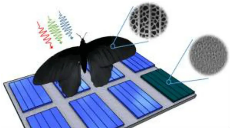
Butterfly wing nanostructures created on solar cells, improves efficiency by 200 per cent
On November 16, 2017 by AnilResearchers have achieved a breakthrough by replicating nanostructures discovered on butterfly wings in solar cells, boosting their light absorption capability by up to 200%. The study, featured in the journal Science Advances, addresses the issue of sunlight reflected by solar cells being wasted as unused energy. The nanostructures on the wings of the Pachliopta aristolochiae butterfly, characterized by nanoholes, enable superior light absorption across a broad spectrum compared to smooth surfaces.
The butterfly, known for its deep black hue, signifies optimal sunlight absorption for effective heat management, as explained by Hendrik Holscher from the Karlsruhe Institute of Technology (KIT) in Germany. The team of scientists, fascinated by the butterfly’s mechanisms, successfully replicated its nanostructures within the silicon-absorbing layer of a thin-film solar cell.

The absorption rate of incident light perpendicular to the surface increased by 97% compared to a smooth surface. This rate continued to rise, reaching 207% at an angle of incidence of 50 degrees. This is particularly relevant in European conditions where diffuse light often falls on solar cells at non-vertical angles, according to Holscher.
However, Guillaume Gomard of KIT emphasized that the theoretical 200% efficiency enhancement does not necessarily translate to a proportional increase in the overall efficiency of the entire photovoltaic (PV) system. Other system components also play a role in determining efficiency.

Before implementing the nanostructures in solar cells, the researchers used scanning electron microscopy to determine the diameter and arrangement of the nanoholes on the butterfly wing. They conducted a computer simulation to analyze the rates of light absorption for various hole patterns, discovering that disordered holes of varying diameters, similar to those on the black butterfly, yielded the most stable absorption rates across the entire spectrum and at variable angles of incidence. The researchers introduced disorderly positioned holes with diameters ranging from 133 to 343 nanometres in a thin-film PV absorber.
Calendar
| M | T | W | T | F | S | S |
|---|---|---|---|---|---|---|
| 1 | ||||||
| 2 | 3 | 4 | 5 | 6 | 7 | 8 |
| 9 | 10 | 11 | 12 | 13 | 14 | 15 |
| 16 | 17 | 18 | 19 | 20 | 21 | 22 |
| 23 | 24 | 25 | 26 | 27 | 28 | 29 |
| 30 | 31 | |||||